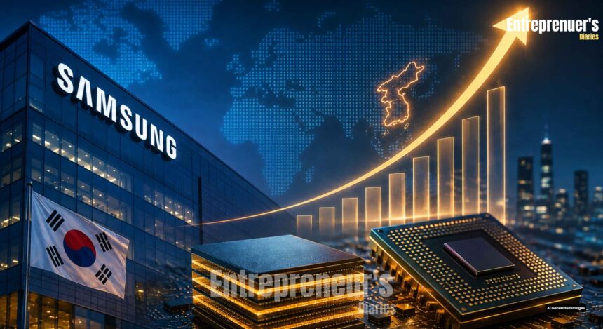
Seoul, South Korea, June 26, 2026: Six hundred and forty eight billion dollars isn’t a rounding error. It isn’t a budget adjustment made during a quiet quarterly earnings call. When you hear a financial commitment that massive attached to a single industry, you have to stop and ask what exactly is driving the panic. Because make no mistake, this kind of money isn’t deployed from a position of comfortable dominance.
- Samsung Investment: Unpacking the National Blueprint Behind the $648 Billion Bet
- The Cultural Earthquake: Admitting You Are Losing
- The Plumbing Problem: Why AI Needs a New Kind of Memory
- The One Stop Shop Gambit
- Pouring Concrete in Yongin
- The Geopolitical Minefield
- Looking Over Their Shoulder
- Why This Bet Could Still Fail
- The Founder’s Playbook: What You Can Actually Learn
- The Analytical Closing: Building the Architecture of Tomorrow
- Frequently Asked Questions
The latest Samsung Investment plan shows what happens when one of the world’s biggest technology companies believes the future of artificial intelligence and semiconductors demands an unprecedented long term commitment. It’s deployed when a company realizes the ground beneath its feet is turning to quicksand.
According to an official press release from the South Korean Ministry of Trade, Industry and Energy, the country’s private sector, anchored by Samsung Electronics and SK Hynix, has just unveiled a staggering 900 trillion won ($648 billion) investment blueprint. The target? The semiconductor ecosystem. The timeline? Stretching all the way to 2047.
For anyone running a business, from a scrappy startup to a mid market enterprise, you might be tempted to scroll past this headline. It feels too big, too distant from the reality of your own P&L statement. But that would be a mistake.
Strip away the staggering zeroes and the geopolitical posturing, and what you have is a masterclass in corporate survival. It is a textbook example of how a legacy giant reacts when a structural shift in technology threatens to render its core business model obsolete.
Let’s break down what is actually happening, why Samsung’s leadership essentially sounded the alarm bells, and what this bet tells us about the future of global business.
Samsung Investment: Unpacking the National Blueprint Behind the $648 Billion Bet
First, we need to get the facts straight because many headlines oversimplify the announcement. The Samsung Investment making headlines is not a standalone corporate commitment announced solely by Samsung Electronics. Instead, this Samsung semiconductor investment represents a broader national strategy.
According to the South Korean Ministry of Trade, Industry and Energy, the $648 billion (900 trillion won) figure represents a long term national investment blueprint led by the country’s private semiconductor sector, with Samsung Electronics and SK Hynix serving as its primary driving forces.
The strategy extends through 2047 and includes 340 trillion won dedicated to semiconductor research and development, according to the ministry. The investment is also expected to strengthen Samsung AI chips development as artificial intelligence infrastructure becomes a long term strategic priority.
Samsung remains the central force behind this broader national plan. While the company has not disclosed its exact share of the 2047 investment blueprint, it previously announced a separate 450 trillion won semiconductor investment program covering 2022 through 2026, making Samsung investment 2026 an important milestone in the company’s broader semiconductor strategy.
The latest national framework goes far beyond that earlier commitment by extending the investment horizon for more than two decades. For business leaders, this shift is more significant than the headline figure itself. It signals that Samsung is no longer planning around traditional semiconductor cycles but around a long term belief that artificial intelligence infrastructure will reshape the future of computing for decades to come.
The Cultural Earthquake: Admitting You Are Losing
To understand the gravity of this pivot, you have to understand the culture of South Korean conglomerates, known as chaebols. Historically, these organizations do not air their dirty laundry in public. Admitting a strategic failure to the outside world is taboo.
Which is why the recent statements from Samsung’s leadership were so jarring. During the company’s annual shareholder meeting in March 2024, Vice Chairman and Head of the Device Solutions Division, Jun Young hyun, took the stage. According to verified reporting by Reuters and the Financial Times, he didn’t mince words.
“The circumstances are very serious,” Jun stated. “We need to make fundamental changes.” He openly acknowledged that Samsung was lagging behind its competitors in the AI semiconductor race.
A few weeks later, at an internal company event covered by the Associated Press, Jun doubled down. He told his executives that Samsung’s future had to be built on “super gap” technologies advancements so massive that competitors simply couldn’t copy them.
This is a crucial strategic indicator. When a newly appointed leader publicly lowers the baseline of expectations, they are deliberately breaking the internal status quo. You don’t tell shareholders you are losing unless you are preparing them for a massive, costly, and disruptive strategic pivot.
Jun was clearing the runway. He was making it culturally acceptable to spend hundreds of billions of dollars to fix a problem that, until recently, Samsung pretended didn’t exist.
The Plumbing Problem: Why AI Needs a New Kind of Memory
To grasp why Samsung is in trouble, you have to look past the software of artificial intelligence and look at the hardware. For the last few decades, Samsung absolutely dominated the world in commodity memory specifically DRAM and NAND flash. These are the chips that store data in your laptop and your phone.
The business model was brutal but simple. You build massive fabs. You drive down the cost per gigabyte. You survive the inevitable boom and bust cycles where oversupply crashes prices. Generative AI broke that model.
AI models don’t just need storage; they need speed. When an AI model like ChatGPT is generating a response, the logic processor (the brain) needs to be fed massive amounts of data instantaneously. If the memory can’t keep up, the incredibly expensive processor just sits there, waiting. It’s a plumbing problem. You can have the world’s most powerful showerhead, but if the pipes leading to it are the size of a straw, you’re not getting much water.
This technical requirement elevated a niche technology called High Bandwidth Memory, or HBM, to the most critical component in the AI server supply chain. HBM works by stacking multiple layers of memory vertically, connecting them with microscopic wires called Through Silicon Vias (TSVs). This vertical stack sits right next to the AI processor, allowing for massive, instantaneous data transfer.
And here is where Samsung stumbled. According to TrendForce, a globally recognized semiconductor research firm whose data is frequently cited by Bloomberg, SK Hynix Samsung’s domestic rival captured an estimated 50% to 60% share of the HBM market in late 2023 and early 2024.
Samsung, the historical king of memory, was left in the dust. Nvidia, the company making the AI processors that are driving the global tech rally, overwhelmingly relies on SK Hynix for these critical HBM chips. Losing that market share isn’t just a temporary hit to revenue. It’s a fundamental threat to Samsung’s identity.
The One Stop Shop Gambit
So, how does Samsung fight back? Throwing money at the problem is part of it, but capital alone doesn’t guarantee a technological catch up. Samsung has to play a different game. And they believe they have an ace up their sleeve: vertical integration.
If you look at the competitive landscape right now, the supply chain is incredibly fragmented. Taiwan Semiconductor Manufacturing Company (TSMC) dominates the foundry business. They manufacture the advanced logic chips (the brains) designed by companies like Nvidia and Apple. But TSMC doesn’t make memory.
SK Hynix makes the memory, but they don’t operate a major foundry to make the logic chips. So, to build an advanced AI processor, a company like Nvidia has to get the logic chip from TSMC, the memory from SK Hynix, and then pay TSMC to perform advanced packaging to physically stick them together.
According to official Samsung investor presentations, Samsung is the only major player on earth with top tier competitive capabilities in both advanced memory manufacturing and contract foundry manufacturing.
Their strategic bet is to offer a “turnkey” solution. Instead of making customers juggle a fragmented supply chain, Samsung wants to manufacture the logic chip and the HBM under one corporate roof, co-optimizing the designs to squeeze out better performance and lower power consumption.
If they can pull this off, they aren’t just selling a component anymore. They are selling a complete architecture. This is a massive strategic pivot. It changes Samsung’s bargaining power with hyperscale cloud providers like Amazon, Microsoft, and Google. If you can reduce a customer’s integration friction, you can command higher margins and secure longer term contracts.
Pouring Concrete in Yongin
A strategy of this magnitude can’t just live on a PowerPoint. It requires an obscene amount of physical infrastructure. According to the official Samsung Electronics Newsroom, the physical manifestation of this bet is the Yongin Semiconductor Cluster. Located south of Seoul, this site is described by the company as the largest single semiconductor manufacturing complex ever conceived.
The scale is genuinely hard to wrap your head around. Samsung states the total site area spans over 7.1 million square meters. That is roughly the size of 1,000 soccer fields. The phased construction plan involves building four advanced fabrication plants, alongside dedicated facilities for the advanced packaging we just discussed, plus research and development centers.
The first phase of this mega cluster is officially slated for completion and mass production in 2027. From an operational standpoint, the Yongin cluster is a bet on agglomeration economics. By forcing R&D and manufacturing to exist on the exact same patch of dirt, Samsung is trying to destroy the time it takes to move a chip from a design concept to high volume manufacturing.
In the hyper competitive AI market, speed to market is a lethal weapon. Furthermore, centralizing the ultra pure chemicals, water, and power required for advanced manufacturing offers massive cost advantages at scale. They are literally trying to build an impenetrable physical fortress of silicon.
The Geopolitical Minefield
Of course, no corporate strategy of this size exists in a vacuum anymore. Semiconductors are no longer just consumer electronics; they are the new oil, and the new weapons. According to official publications from the U.S. Department of Commerce, the United States has implemented aggressive export controls designed to choke off China’s access to advanced AI chips and the equipment needed to make them.
Simultaneously, the U.S. CHIPS and Science Act is throwing billions of dollars in subsidies at companies willing to build fabs on American soil. But there is a catch. A very sharp catch.
According to official U.S. government disclosures, the CHIPS Act funding comes with strict “guardrail” provisions. If you take the money, you are legally prohibited from expanding or upgrading your advanced semiconductor manufacturing capacity in China for a decade.
Samsung, which has historically operated major manufacturing facilities in China to serve the local market, has found itself in a geopolitical vise. They recently accepted $6.4 billion in direct funding from the U.S. CHIPS Act to build a massive foundry in Taylor, Texas.
This explains a lot of the motivation behind the $648 billion domestic investment in South Korea. Because they are legally restricted from expanding their most advanced tech in China, and because relying entirely on the U.S. introduces its own set of political risks, Samsung must aggressively build out its sovereign, domestic South Korean infrastructure. The Yong in cluster isn’t just a business decision. It’s a geopolitical insurance policy.
Looking Over Their Shoulder
Samsung is swinging for the fences, but their rivals aren’t exactly standing still SK Hynix knows that Samsung’s vertical integration play is a direct threat to their HBM dominance. According to reporting by CNBC, SK Hynix’s CEO, Kwak Noh jung, stated in early 2024 that his company plans to mass produce next generation HBM chips ahead of schedule. Their strategy is simple: run so fast that Samsung’s integrated model can’t catch up.
TSMC, the foundry giant, sees the threat too. They aren’t going to start making memory, but according to official TSMC publications and industry analysis, they are advancing their own packaging technologies to standardize how third party memory (like SK Hynix’s) connects to their logic chips.
They are trying to make the fragmented supply chain work so smoothly that customers don’t feel the need to switch to Samsung’s one stop shop. Then there is Intel. Backed heavily by U.S. subsidies, Intel is attempting a massive turnaround to become a major foundry player again. While they are currently behind in the AI race, you can never count out a company with that much resources and government backing.
The landscape is an absolute arms race. And in an arms race, the entity with the deepest pockets usually wins if they can avoid shooting themselves in the foot.
Why This Bet Could Still Fail
It is easy to look at a $648 billion plan and assume victory is inevitable. It isn’t. The execution risks here are terrifying, and business leaders should study them closely. First, there is the brutal reality of advanced packaging yields. Stacking memory chips vertically and connecting them with microscopic wires is incredibly difficult.
If Samsung’s manufacturing lines produce a high percentage of defective chips, their costs will skyrocket. You can have the best architectural strategy in the world, but if your factory yields are garbage, your margins are toast.
Second is the threat of overcapacity. The semiconductor industry has a nasty habit of building massive fabs just as demand dries up. If the current frenzy around generative AI cools down either because enterprise adoption slows or because software becomes more efficient and requires fewer chips Samsung will be stuck with incredibly expensive, empty factories. That is a fast way to destroy shareholder value.
Finally, there is the human element. According to the South Korean government’s own assessments accompanying this investment blueprint, the country faces a critical, severe shortage of semiconductor engineers. You can pour concrete endlessly, but if you don’t have the thousands of Ph.D. level talents required to run 2 nanometer equipment, those fabs are just very expensive tombs.
The Founder’s Playbook: What You Can Actually Learn
Okay, let’s bring this back down to earth. You aren’t building a $648 billion semiconductor cluster. So why does this matter to you?
Because the strategic mechanics Samsung is using are highly scalable, even if the budget isn’t.
Use disproportionate scale to reset the clock.
When a competitor catches you flat footed, you cannot win by tweaking your existing product. You have to make the game so expensive to play that they can’t keep up. Samsung is using capital to raise the barrier to entry.
As a smaller business, you might not have financial capital, but you have other forms of capital. Can you invest so heavily in a specific niche technology, or a specific customer service model, that it becomes financially unviable for your competitors to copy you? Force a reset of the rules.
Sell the ecosystem, not the component.
This is the vertical integration play. Tech markets mature, and customers get tired of hiring three different vendors to make a system work. They just want the outcome.
Look at your own business. Are you selling a single piece of software, or are you selling the solution to the customer’s entire workflow? The company that absorbs the most complexity for the customer usually wins the highest margins.
Honesty is a strategic weapon.
Remember Jun Young hyun telling the world Samsung was lagging? That was intentional. In your own company, middle management will always hide bad news to protect their bonuses. If you want to pivot your business, you have to create a culture where admitting failure is rewarded, because it’s the only way to get the organization to accept the painful changes required to fix it.
Align your growth with macro forces.
Samsung didn’t just announce a tech plan; they tied it to South Korea’s national security and economic agenda. They are going to get tax breaks, fast tracked permits, and government backing.
Are you fighting regulatory headwinds, or are you aligning your growth strategy with government incentives, sustainability grants, or massive demographic shifts? Ride the wave, don’t swim against it.
The Analytical Closing: Building the Architecture of Tomorrow
When historians look back at this era of business, they won’t care about the marketing funnels we optimized or the SaaS tools we launched. They will look at the physical infrastructure we chose to build. Samsung’s role in this $648 billion blueprint isn’t just a reaction to a trending topic. It is a profound, almost desperate belief about the future architecture of computing.
They are betting that AI will not stay trapped in massive, centralized cloud servers. They are building the physical capacity to put high bandwidth, low power intelligence into autonomous vehicles, edge devices, and robotics markets that barely exist today but will define the next thirty years of the global economy.
What separates this strategy from ordinary corporate planning is the total rejection of short termism.
We live in an era obsessed with quarterly earnings, immediate ROI, and quick exits. Committing to a 23 year capital deployment plan is an act of aggressive corporate conviction. It requires a leadership team willing to endure years of skeptical investors and massive execution risk to secure a position of dominance in a market that doesn’t quite exist yet.
That is the ultimate lesson for anyone running a business. True competitive advantage is rarely won in the light of present day certainty. It is forged in the dark, by those willing to build the infrastructure for a world they can clearly see, long before the rest of the market wakes up and realizes the ground has shifted beneath them.
Samsung isn’t just spending money to make chips. They are spending it to ensure the future of artificial intelligence runs on an architecture they own. That is the benchmark of ambition. The only question left is whether they can actually pull it off.
Frequently Asked Questions
What exactly is the $648 billion Samsung investment plan?
According to the South Korean Ministry of Trade, Industry and Energy, the $648 billion (900 trillion won) figure is a national investment blueprint spanning to 2047. It involves the private sector driven primarily by Samsung Electronics and SK Hynix allocating funds for semiconductor research, development, and manufacturing infrastructure. Samsung is the anchor of this plan, though the total number represents the combined national effort.
Why is Samsung suddenly investing so heavily in High Bandwidth Memory (HBM)?
High Bandwidth Memory is the critical component that prevents AI processors from stalling out due to slow data transfer. According to market data from TrendForce, as reported by Bloomberg, Samsung’s rival SK Hynix currently holds over 50% of the HBM market. Samsung’s massive investment is a strategic emergency maneuver to close this gap and reclaim leadership in the most profitable segment of the memory market.
How does Samsung’s strategy differ from its main competitor, TSMC?
Unlike Taiwan Semiconductor Manufacturing Company (TSMC), which dominates the manufacturing of logic chips but relies on third parties for memory, Samsung has top tier capabilities in both. According to official Samsung investor presentations, their strategy is vertical integration offering clients a turnkey solution where both the AI logic chip and the HBM are co-optimized and manufactured under one roof.
What is the Yongin Semiconductor Cluster?
According to the official Samsung Electronics Newsroom, the Yongin cluster is a massive 7.1 million square meter manufacturing site south of Seoul. It is designed to be the largest single semiconductor complex in the world, housing multiple advanced fabrication and packaging facilities. It is the physical center piece of Samsung’s long term strategy to accelerate speed to market for AI chips.
How do U.S. regulations impact Samsung’s global strategy?
According to the U.S. Department of Commerce, companies receiving funding from the U.S. CHIPS Act are strictly prohibited from expanding advanced semiconductor capacity in China. Because Samsung accepted $6.4 billion in U.S. funding for a Texas foundry, they are legally restricted in China. This forces Samsung to invest heavily in domestic South Korean infrastructure like the Yongin cluster to maintain a secure, sovereign manufacturing base.
Connect With Us On Social Media [ Facebook | Instagram | Twitter | LinkedIn ] To Get Real-Time Updates On The Market. Entrepreneurs’ Diaries Is Now Available On Telegram. Join Our Telegram Channel To Get Instant Updates.

Isabella is a global business journalist and former McKinsey analyst from Brazil. She brings sharp insights on economic shifts, policies, and founder journeys from around the world.

Freya is a digital nomad and writer from Sweden, curating business travel hacks and remote-work inspiration from her global adventures.